The march toward ever-smaller semiconductor nodes has brought remarkable advancements in computing power, efficiency, and integration. But it has also brought unprecedented complexity. At dimensions below 5 nanometers, the difference between a functioning chip and a failed one can come down to something as subtle as two metal lines touching or nearly touching on a wafer. These tiny defects, often invisible without specialized tools, can undermine entire batches of chips. Erik Hosler, a semiconductor strategist with a focus on consumer expectations and technology lifecycle alignment, sees this challenge not only as technical but experiential.
In today’s tech environment, the expectation is clear: devices must work seamlessly, reliably, and without compromise. Users are not interested in how many nanometers a process node claims to be. They care about performance, battery life, responsiveness, and stability. That expectation, rooted in user experience rather than process specs, is now the standard that manufacturers must uphold. In this landscape, defect detection becomes not just a process control step, but a cornerstone of product success.
Why Advanced Nodes Are More Vulnerable
As feature sizes shrink, tolerances tighten. At older nodes, slight variances in patterning or alignment might not fail. But at 5 nm and below, there is almost no margin for error. Two conductive lines that even slightly overlap can short-circuit a logic path. A subtle particle embedded in a dielectric can break down insulation. The smaller the feature, the bigger the impact of a tiny defect.
In addition, the complexity of modern chips means that defects may not have immediate or obvious symptoms. Some may manifest only under specific voltage, temperature, or operational conditions. It makes detection during manufacturing even more critical, as post-deployment failures are significantly costlier in terms of both brand trust and revenue.
These risks make high-precision defect detection an essential part of the advanced node process. The challenge is not simply to produce smaller features, but to ensure those features are reliably separated, aligned, and functionally intact.
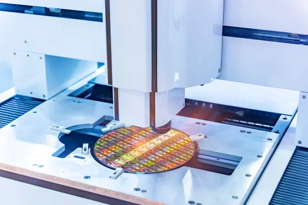
The Role of Metrology and Inspection Tools
To catch defects at these extreme dimensions, manufacturers rely on an increasingly sophisticated toolkit. Traditional optical inspection often lacks the resolution required at sub-5 nm nodes, which is why newer techniques are being introduced.
E-beam inspection, hyperspectral imaging, and Critical Dimension Scanning Electron Microscopy (CD-SEM) provide higher-resolution views of patterns and surfaces. These tools can identify subtle variations in line-edge roughness via alignment and sidewall profile that may indicate a latent defect.
Even more powerful is the integration of machine learning into inspection workflows. By analyzing vast datasets from prior production runs, AI systems can flag defect-prone patterns or statistically significant anomalies, even when they fall within accepted dimensional tolerances.
Defect Detection and Design Feedback
Advanced defect detection doesn’t just protect yield. It also feeds critical insights back into the design process. Engineers can study where failures most often occur, specific geometries, mask transitions, or layer interactions, and use that information to improve future designs.
This feedback loop is especially important in an environment where design complexity outpaces fabrication maturity. For example, if a particular layout consistently leads to bridging defects between metal lines, designers can re-route those areas, adjust spacing, or revise edge profiles.
Such an iterative design-for-manufacturability (DfM) is key to maintaining productivity and reducing scrap. Without timely and detailed defect feedback, design cycles stretch longer, tape-out costs increase, and new product timelines slip.
Process Control at the Atomic Level
At these scales, variability is not just introduced by lithography or etch. It can stem from atomic-scale variations in materials, stochastic resist behavior, or inconsistent deposition thickness. Defect detection systems must be tuned not only to spot faults, but to understand their origin.
That’s why modern fabs pair inspection with inline metrology. Measuring film thickness, line width, critical dimensions, and material composition in real time allows engineers to correlate defect incidence with upstream process variation.
By connecting these dots, fabs can take corrective action before defects propagate downstream. It might mean adjusting a mask alignment, refining an etch profile, or retuning a plasma chamber to improve uniformity.
Defect Detection as a Driver of Experience
From the consumer’s point of view, none of this is visible. What matters is whether the device boots up, the app loads quickly, or the call connects cleanly. That invisible layer of quality is what makes or breaks the user’s impression of the product.
In today’s market, performance is expected to be seamless. Each device can feel faster, more stable, and more intelligent than the last. As engineers know, delivering that experience requires eliminating invisible failures long before the device ever reaches a customer’s hands.
Erik Hosler notes, “So long as that expectation is met, then Moore’s Law, in a sense, is still alive.” Here, “that expectation” is not about transistor density or geometry. It is about delivering an improved, reliable, and consistent user experience with each new generation of technology. And in this new definition, defect detection plays an essential role.
Scaling With Confidence
As the industry prepares to scale toward 2 nm and beyond, the importance of defect detection can only increase. Each new node introduces thinner lines, taller stacks, and more heterogeneous materials. These changes multiply the number of potential failure points.
Rather than being seen as a gatekeeper or bottleneck, defect detection should be viewed as a proactive enabler of progress. It provides the visibility and data required to manage risk, protect yield, and maintain trust in the technology ecosystem. More importantly, it provides the foundation for seamless consumer experiences. In a world where devices are expected to perform flawlessly, that may be the most essential measure of success.
The Line Between Progress and Failure
In the world of advanced semiconductor nodes, success and failure are often separated by only a few nanometers. When two lines touch, the result can be catastrophic. But when the right defect detection systems are in place, those failures can be caught, understood, and eliminated.
Moore’s Law may no longer be about pure scaling. It is about value delivered, performance achieved, and expectations met. Defect detection makes those outcomes possible by ensuring that what was designed is faithfully built, evaluated, and shipped. It is no longer about making mistakes. It is about enabling precision at scale and trust at the consumer level.